


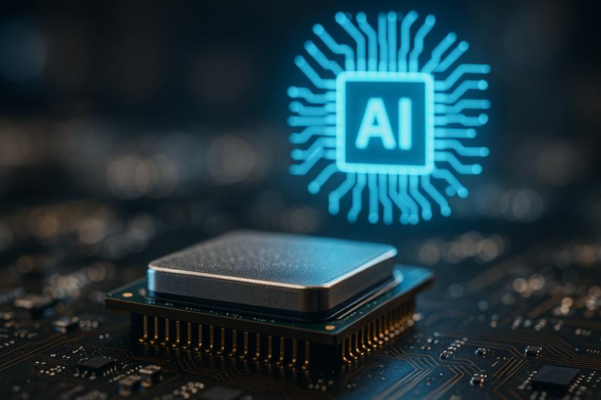
The Role of AI in Hardware Design
The role of Artificial Intelligence (AI) in hardware design is rapidly expanding, particularly in the semiconductor industry where it is revolutionizing development processes. AI-driven tools are transforming semiconductor design workflows by enabling layout generation, design optimization, and defect prediction. These advances are significantly accelerating time-to-market for new chips and devices, fostering innovation at an unprecedented pace. Learn more about the innovations driven by AI in the semiconductor industry at Aegis Softtech.
Beyond conventional design improvements, AI is instrumental in the discovery and synthesis of novel semiconductor materials, including advanced 2D materials and quantum dots. These materials hold the key to future generations of electronics, promising miniaturization and enhanced processing capabilities that align with growing demands for efficiency and performance. The increasing adoption of AI in semiconductor development reflects its powerful ability to handle complex design challenges, reduce errors, and optimize functionality while cutting costs and development cycles. This trend underscores AI's significance as a transformative force that is setting new standards in hardware engineering and semiconductor innovation.
Machine Learning Integration in Chip Design
Machine learning (ML) algorithms are increasingly integrated into multiple stages of the chip design process to enhance efficiency and performance. In architecture optimization, ML models analyze vast design parameters to suggest innovative configurations that maximize speed and reduce power consumption. This automated insight helps engineers explore more design alternatives quickly, leading to better-performing chips. The impact of AI and machine learning in chip design explains resource savings and architectural improvements.
During layout planning, ML assists by predicting optimal component placement and routing paths. This reduces signal delay and cross-talk, improving overall chip functionality. Machine learning models can also identify potential design failures early, minimizing costly iterations. Overall, integrating machine learning in chip design accelerates verification processes, targets high-risk design areas for testing, and optimizes resource use, resulting in faster development cycles and improved chip quality.
Advantages of AI in Hardware Design
Utilizing artificial intelligence (AI) in hardware design offers several key advantages that significantly enhance the development process and end-product quality. One of the primary benefits is faster development cycles. AI-driven design tools can automate complex tasks such as circuit layout and component placement, reducing the time engineers spend on repetitive manual work. This acceleration enables quicker prototyping and iteration, bringing hardware products to market more rapidly. According to InTechHouse's overview of AI in hardware design, AI-driven design can significantly reduce design time and errors, leading to more efficient and cost-effective hardware solutions.
Another critical advantage is the minimization of errors. AI algorithms can analyze vast amounts of design data to detect potential faults or inefficiencies early in the design phase, preventing costly mistakes downstream. This predictive analysis helps ensure higher reliability and robustness of hardware components before fabrication. Furthermore, AI enables the creation of high-performance chips through advanced optimization techniques. By exploring vast design possibilities that may be impractical for human designers to assess, AI can discover innovative configurations that maximize performance, reduce power consumption, and optimize resource usage.
Google's TPU: A Case Study in AI-Driven Chip Development
Google's Tensor Processing Unit (TPU) is a prime example of AI-driven innovation in chip development, designed specifically to accelerate machine learning workloads. Introduced in 2016, the TPU architecture is optimized for TensorFlow operations and enables faster training and inference of deep learning models compared to traditional CPUs and GPUs. Iterations of the TPU, such as TPU v4 and the latest TPU v5p, have continually improved performance with increased memory bandwidth and computational speed, making them critical for powering Google’s AI services including search, translation, and conversational agents.
The tangible benefits of using TPUs in chip development include significantly reduced processing times for complex AI models, improved energy efficiency, and lower operational costs at scale. This specialized hardware has allowed Google to handle vast amounts of data efficiently, enabling rapid AI advancements while maintaining scalable infrastructure. The success of TPUs highlights how integrating AI techniques directly into chip design can revolutionize computing capabilities and drive forward innovation in artificial intelligence. Learn more about Google's Tensor Processing Unit in the detailed Wikipedia overview and explore how Google's TPUs enhance AI workloads in the Google Cloud TPU system architecture documentation.
The Future of AI in Semiconductor Design
AI-driven hardware design is revolutionizing the semiconductor industry, with machine learning playing a crucial role in accelerating innovation and enhancing efficiency. Advanced AI-powered Electronic Design Automation (EDA) tools are automating repetitive tasks such as schematic generation and layout optimization, significantly reducing the time required for chip design. Looking ahead, these AI technologies are expected to transform the semiconductor sector by enabling automated place-and-route operations and smarter manufacturing processes. For instance, tools like Synopsys' DSO.ai have demonstrated the capability to cut the design timeline for cutting-edge 5nm chips from several months to just a few weeks.
Beyond design, AI's influence extends to optimizing supply chains and fostering sustainable industry practices. However, these advancements come with challenges related to data privacy, intellectual property protection, and the need for collaborative innovation. As machine learning continues to evolve, its integration with hardware design promises to drive faster development cycles, more efficient chips, and ultimately, a more intelligent semiconductor ecosystem poised for rapid growth leading into 2030 and beyond. Learn more about how AI is transforming the semiconductor industry in 2025 and beyond from Straits Research.
Sources
- Aegis Softtech - AI in Semiconductor Industry
- Google Cloud - TPU System Architecture Documentation
- Wikipedia - Tensor Processing Unit
- InTechHouse - AI in Hardware Design
- World Journal of Advanced Research - The Impact of AI and Machine Learning in Chip Design
- Straits Research - AI is Transforming the Semiconductor Industry
